Routing a Power Inverter Design Guidelines
前言
客戶在馬達控制設計上常常會有layout上問題,但這邊很多是個架Know How,這邊ST提供重點關鍵設計指引避免在馬達控制上設計踩坑,最後導致ADC回授電路雜訊過多干擾實際馬達控制,另外也提供MOS設計規範指引讓客戶指引可以知道後續設計要點
Circuit loops Guidelines
基本上最重要一個要點就是避免大區域Loops設計(Avoid big area loops as much as possible!)
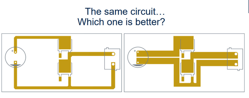
- Loops on the PCB are acting as coils
- The bigger loop area, the bigger issue
- Circuit with bigger area loop:
- Generates noise (e. g. switching of the transistors)
- Absorb noise (e. g. shunt signal feedback)
- Focus on complete loop: from source to load and
back to the source - Keep the area of the loops as small as possible!
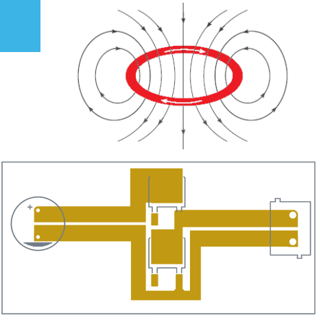
Good component placement is the key
- By optimal components placement the routing
- can be easier
- Study the schematic first and decide what blocks
should be close to each other - There is no ideal placement!
Always compromise between general rules,
specifics of the inverter, manufacturing limits, etc.
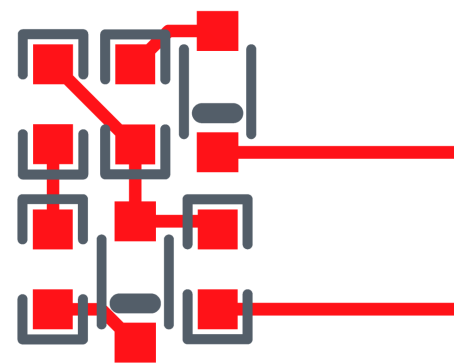
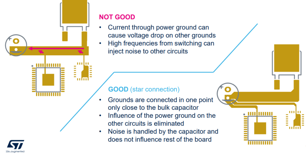
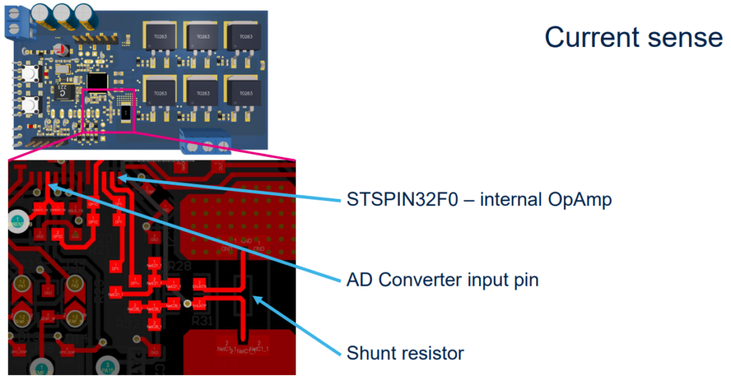
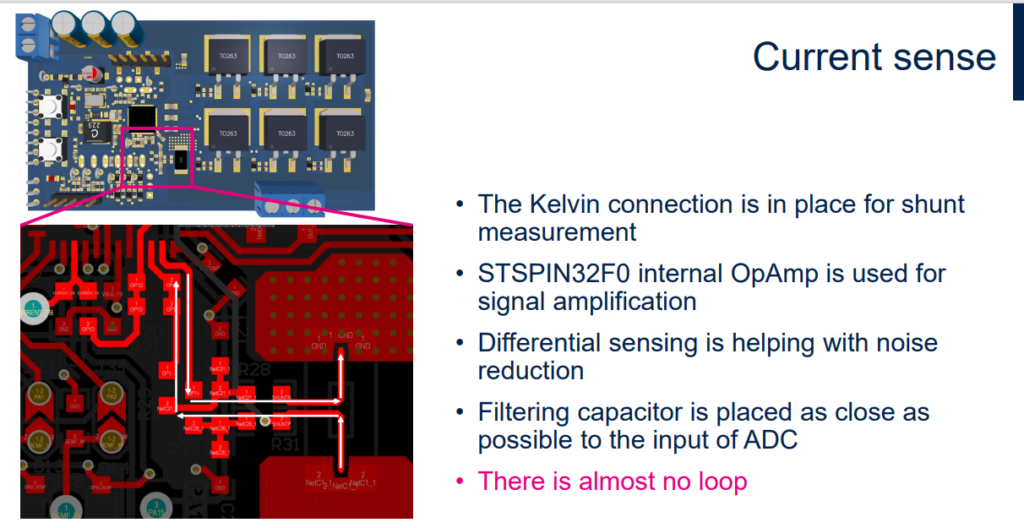
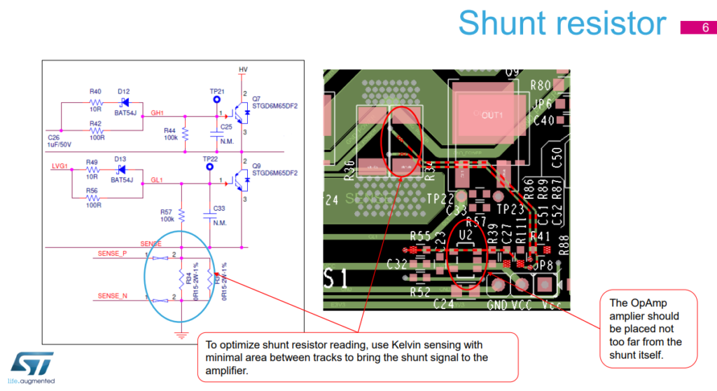
連接方式會建議使用 Kelvin connection/Star Connection
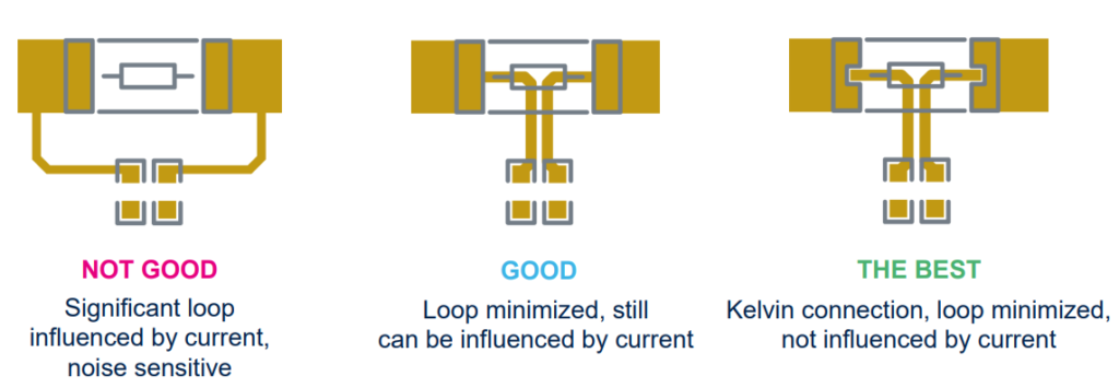
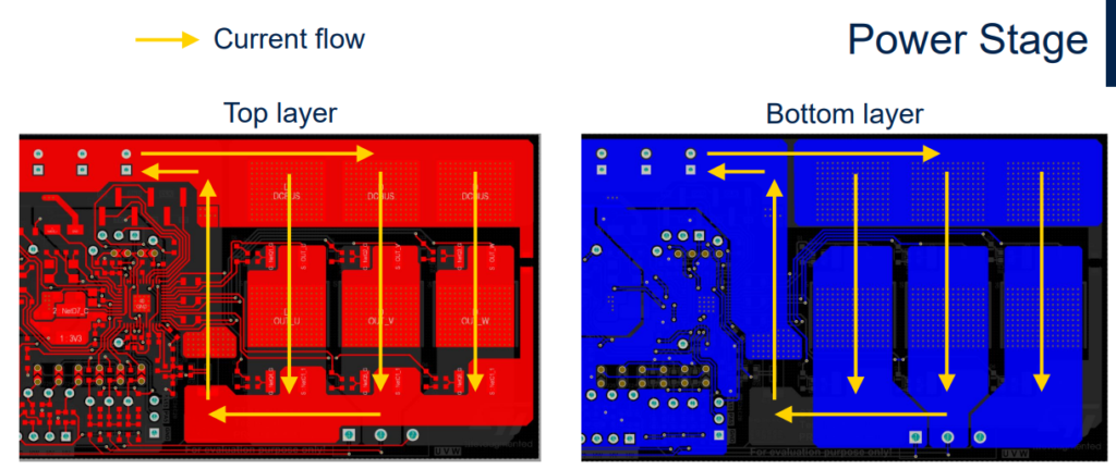
範例
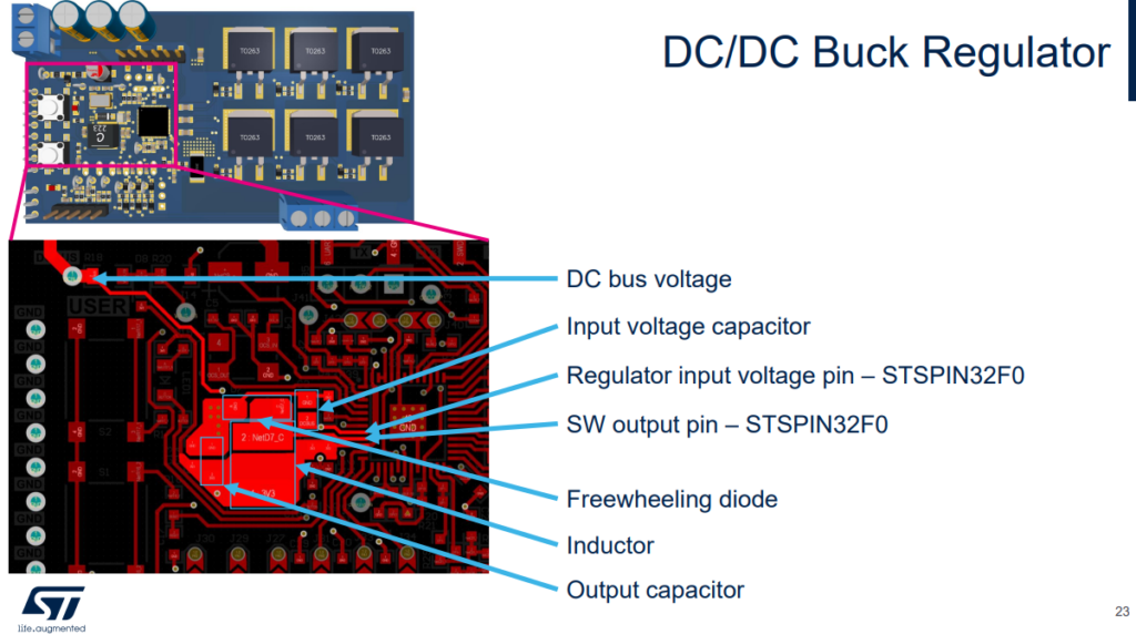
Current loop area is minimized and there are no sensitive circuits inside it
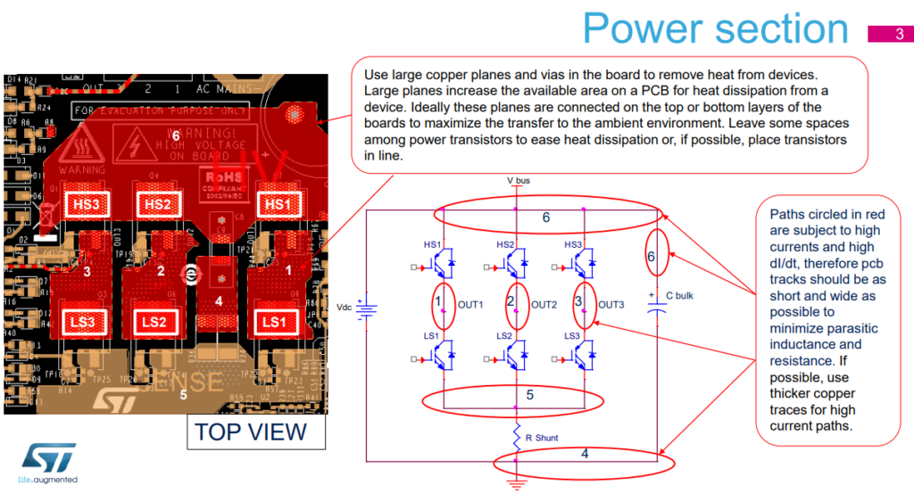


GND設計上會建議分開數位GND還有Power GND
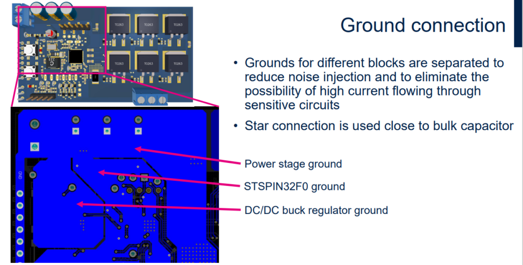
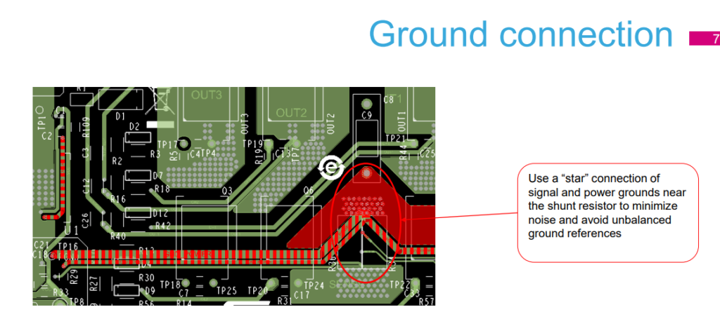
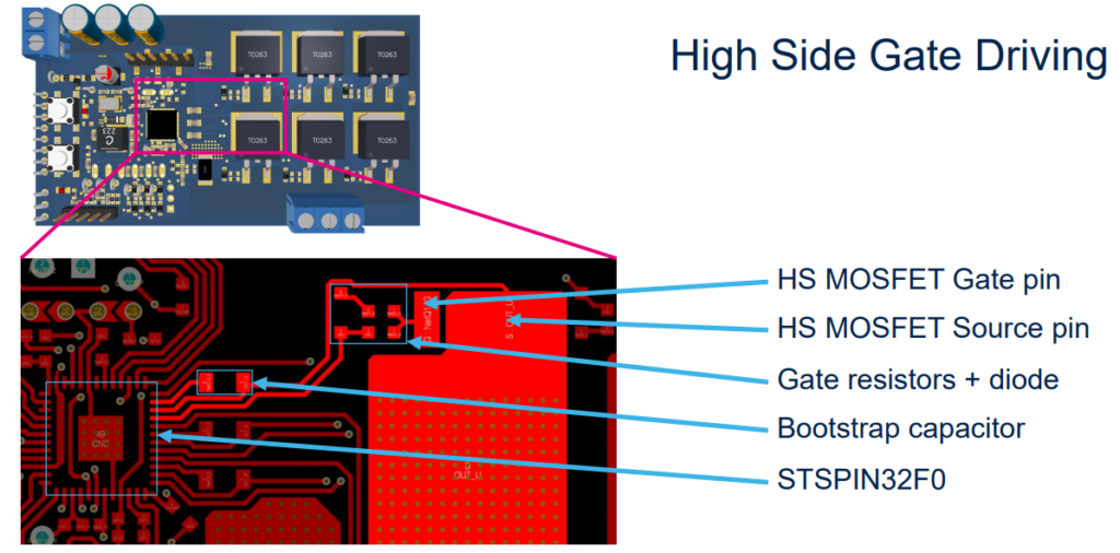
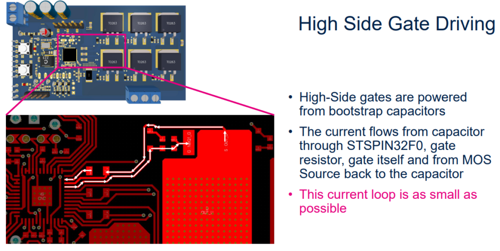
其他MOS等設計可以參考下面文件Power MOSFETs: best choice guide for VRM applications

博主您好
這篇文章有關於STSPIN32F0的設計指引
請問是截自官方的哪一份投影片呢?
Routing a Power Inverter around STSPIN32F0
Motor Control Application Lab
博主您好
這篇文章中有關STSPIN32F0的設計指引
請問是截自哪一份官方投影片呢?